Difference between revisions of "SNES2Atari"
| Line 120: | Line 120: | ||
==Authorship== | ==Authorship== | ||
| − | The SNES2Atari circuit design and adapter was written by AtariAge user Danjovic. All code and | + | The SNES2Atari circuit design and adapter was written by AtariAge user Danjovic. All code and circuit design was kindly provided by him under the "no rights reserved" CC0 license. |
Revision as of 16:18, 19 November 2022
What is it?
The SNES2Atari is an adapter that allows you to connect an SNES controller to the Atari 7800, 2600, the Atari 8-bit computer line, and likely many other platforms that have a DB9 joystick port and can use Atari joysticks. Games must be specifically coded to use the SNES controller.
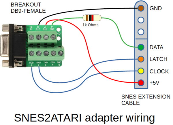
The design is quite minimal, and can be implemented with just an snes extension cable, a 1kΩ resistor, and a serial DB9 breakout connector. Alternatively, a more robust adapter can be implemented with a minimal pcb, an snes port, a 1kΩ resistor, and a serial DB9 connector.
The SNES2Atari circuit and driver was created AtariAge user Danjovic.
SNES2Atari Adapter Wiring
SNES2Atari Driver
 ;    ___ _  _ ___ ___      _     _
 ;   / __| \| | __/ __|  __| |_ _(_)_ _____ _ _
 ;   \__ \ .` | _|\__ \ / _` | '_| \ V / -_) '_|
 ;   |___/_|\_|___|___/ \__,_|_| |_|\_/\___|_|
 ;
 ; SNES controller on port 2
 ;      V2 - Detect SNES controller

 ;  Connections
 ;  Atari                SNES
 ;                      +---+
 ; VCC   (7)-+----------| o | VCC
 ;  UP   (1)------------| o | CLOCK
 ; DOWN  (2)------------| o | LATCH
 ; FIRE  (6)----vvvv----| o | DATA
 ;             1k Ohm   +---+
 ;                      | o |
 ;                      | o |
 ; GND   (8)-+----------| o | GND
 ;                      '._.
 ; LEFT  (3)- n.c.
 ; RIGHT (4)- n.c.
 ; POT1  (5)- n.c.
 ; POT2  (9)- n.c.
 ;


 ; initialize port 2 and detect controller
 ; return zero flag activated if controller detected

INITPORT2:
   lda SWCHB
   ora #$10
   sta SWCHB  ; PB4 High->DISABLE transistor Q5, enabling single button joystick

   ;jmp SMPSN1 ; finish initialization

   lda #$03         ; 2
   sta CTLSWA       ; 5 enable pins UP/DOWN to work as outputs
   sta SWCHA        ; 5 make pins clock (UP) and latch (DOWN) to go high
   rts              ; 6

 ; detect controller
 ; return carry set if fail
DETECT:
   jsr SAMPLESNES
   bcs END_DETECT
   lda LowDataByte  ; bits 16 15 14 13 12 11 10 09
   ora #$0f         ; bits 16 15 14 13 Hi Hi Hi Hi  all Hi's for SNES controller
   eor #$ff         ; shall be all Low's for SNES controller
   beq END_DETECT
   sec ; set carry to indicate no controller detected
END_DETECT:
   rts

 ; sample controller on port 2
 ; assume port already initialized
 ; At the end:     7     6    5    4    3     2     1    0
 ; LowDataByte:    1     1    1    1   RSH   LSH    X    A
 ; HighDataByte: RIGHT LEFT DOWN  UP  START SELECT  Y    B
 ; Carry Flag is the 17th bit
 ;
SAMPLESNES:         ; 6 (from jsr)
   lda #$0          ; 2 clock down, latch down
   sta SHWCHA       ; 4 make both latch and clock down
   ldx #$01         ; 2 clock up, latch down
   ldy #16          ; 2 16 bits
   lda #$ff         ; 2 Initialize with no button pressed
   sta LowDataByte  ; 5 if necessary to gain a few microseconds
   sta HighDataByte ; 5 from latch/clk down till first bit sample
   lda #$0          ; 2
SMPSN0:
   rol INPT5        ; 5 sample data
   stx SWCHA        ; 5 clock up
   ror LowDataByte  ; 5 take some time assume
   ror HighDataByte ; 5
   sta SWCHA        ; 4 clock down
   dey              ; 2 next bit
   bne  SMPSN0      ; 2 repeat

   stx SWCHA        ; 5 clock up, next edge  to read 17th bit
   rol INPT5        ; 5 sample data, 17th bit on Carry
   lda #$03         ; 2 both clock and latch up
   sta SWCHA        ; 5 finish sampling
   rts              ; 6


 ; Total time take for sample, from jsr SAMPLE till return:
 ; 6+2+4+2+2+2+5+5+2 + 16* (5+5+5+5+4+2+2) + 5+5+2+5+6
 ; 30                + 16* (28)            + 23
 ; 30                + 448                 + 23  = 501 cycles  =~421us at 1.19MHz

 ;clocks:
 ;____           ___       ___       ___       ___
 ;    \_______s_/   \___s_/   \___s_/   \___s....
 ;____
 ;    \4222552s5/555\422s5/555\422s5/555\422s....
 ;
 ;
 ;from Latch down to read first bit: 4+2+2+2+5+5+2 = 22 -> 18.5us
 ;from clock rise to next sample:    5+5+5+5+4+2+2 = 28 -> 23.5us
Authorship
The SNES2Atari circuit design and adapter was written by AtariAge user Danjovic. All code and circuit design was kindly provided by him under the "no rights reserved" CC0 license.
